Lately I've been interested in old computers, I started reading about the 6502, Z80 and 68k and wanted to know how they work and how old computers worked.
I decided to start with the Z80 CPU, but just the CPU through a serial interface seems a bit boring, and graphics too complex right now, so I started reading about old sound chips.
I found the AY-3-8910 PSG (Programmable Sound Generator), it seems it was quite popular and was used by the ZX Spectrum, and you can find it for less than 1€ online, so I decided to buy a couple of them.
They finally arrived along other stuff I bought to build a Z80 computer. I built the Z80 computer on a breadboard but unfortunately there's no more room for cables, and it's not very reliable.
I ordered some PCBs which are yet to arrive, but I want to try out these sound chips already, so I decided to try and do something with an Atmega32.
I decided to use an Atmega32 intead of an Arduino (Atmega328) because that way I can use Serial (UART), SPI, I2C, and still have a full port avaible.

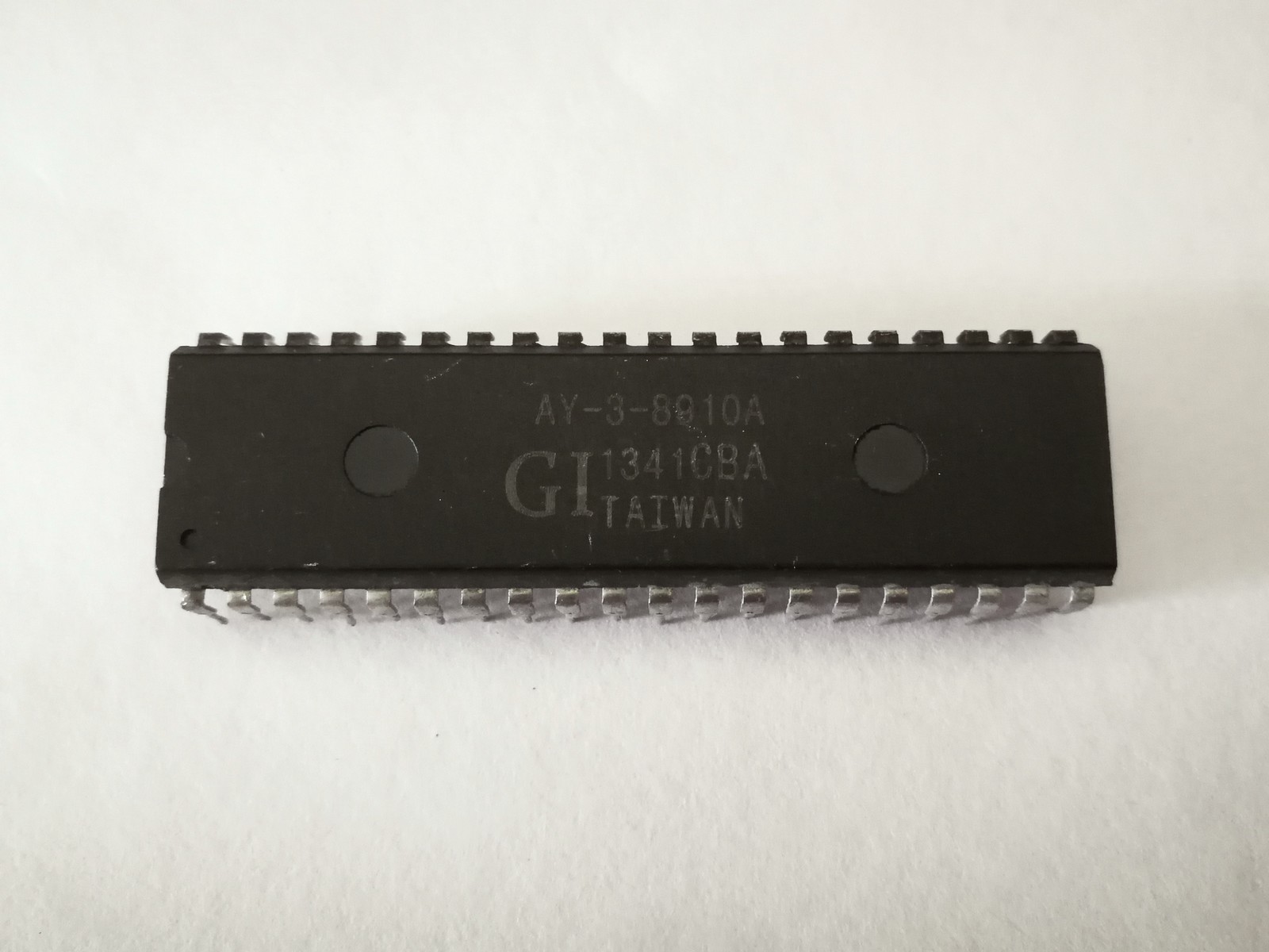
AY-3-8910 received from Aliexpress

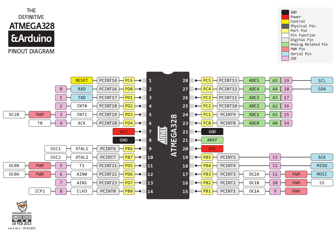
Atmega328 pinout
Wikipedia article:
https://en.wikipedia.org/wiki/General_Instrument_AY-3-8910
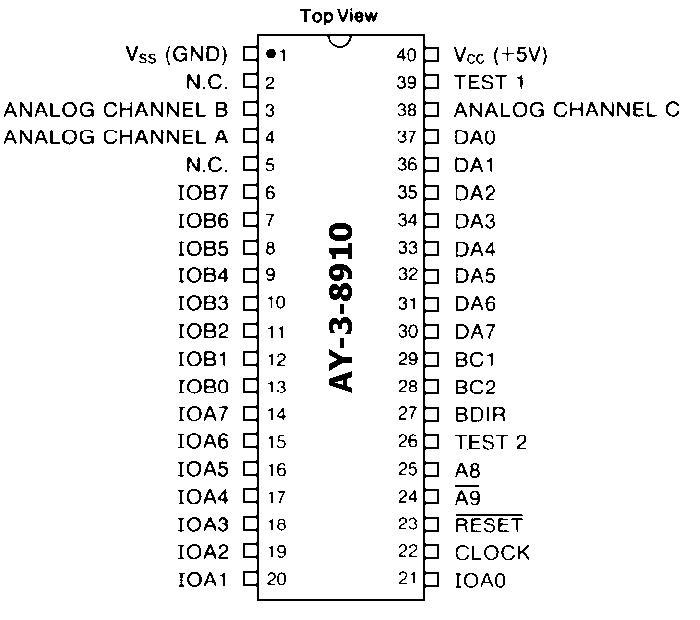
AY-3-8910 pinout:

AY-3-8910 pinout
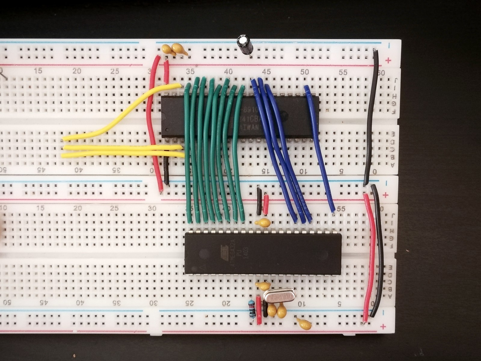
I started connecting everything on a breadboard, I connected the 8-bit data bus (green), 3 control lines (blue), and a clock source (blue) from the Atmega32.
The three yellow cables are the 3 channels, that'll be the audio output. The rest is power, decoupling caps, and a 16MHz crystal for the Atmega32.
AY-3-8910 on breadboard with Atmega32:

AY-3-8910 on breadboard

Atmega32 pinout
The next thing I need is some code, right now writing new code from scratch about something new I don't understand is not something I want to do,
plus, surely someone already wrote code for interfacing this sound chip with an Atmega.
Afer searching a little bit, I found an .ino file that looked good to me:
Code:
https://www.986-studio.com/wp-content/uploads/2014/05/project-ay-3-3910-breadboard.png
The code found is for Arduino/Atmega328, so I have to modify the code for the Atmega32.
Apparently Atmega328 doesn't have a full port except for PORTD, but pins PD0 and PD1 are used for Serial communication (UART).
Atmega328P pinout:
https://ifuturetech.org/wp-content/uploads/2020/04/ATmega328P-PU-PIN-Diagram-connection-configration-scaled-1.jpg
The first part of the code is for the clock generation, this is the new code adapted for Atmega32, it should output 2MHz on pin 15 (PD7).
//Generate 2MHz clock output on pin 15 (PD7) for Atmega32 @16MHz
// Initialize CLK (@ Fosc = 16MHz). clock_freq = (Atmega_clock) / ((OCR2 + 1) * 2)
ASSR &= ~(1 << AS2); // Set Timer2 clock from system clock
TCCR2 |= (1 << CS20); // Set Timer2 clock to "no prescaling"
TCCR2 &= ~((1 << CS21) | (1 << CS22));
TCCR2 |= (1 << WGM21); // Set Timer2 CTC mode
TCCR2 &= ~(1 << WGM20);
TCCR2 |= (1 << COM20); // Set "toggle OC2 on compare match"
TCCR2 &= ~(1 << COM21);
OCR2 = 2; // Set the compare value to toggle OC2 (0 = low or 1 = high)
pinMode(freqOutputPin, OUTPUT); // Set OC2 as output and start to output the clock
Parts of the code read
PORTD = data & 0xFC;
PORTB = data & 0x03;
But what does this mean?
Understanding Atmega port registers
When operating pins on an Atmega chip, 3 registers are used,
DDRx,
PORTx, and
PINx, where 'x' is the port name, A, B, C, D..
DDRx is Data Direction Register, it is used for setting pins as outputs or inputs. (read/write)
Examples:
//Set all PORT A pins as output
DDRA |= 0xFF;
//Set all PORT A pins as input
DDRA |= 0x00;
PINx is a register containing the status of the PORT pins. (read-only)
Examples:
//Input I/O port pins PA7:PA0
InputData = PINA;
PORTx is a register used to change the status of the PORT pins. (read/write)
Examples:
// Turn on I/O port pins Px7:Px0
PORTx = 0xFF;
// Turn on I/O port pin Px only
PORTx |= (1<<Px);
// Turn off I/O port pin Px only
PORTx &= ~(1<<Px);
In short,
PORTx is for outputting data to the pins.
PINx is for reading in data from the pins.
Q: If you can read PORTx, is reading PORTx register the same as reading PINx register?
No, it's not, when you read PORTx register, you're reading the value that's currently set in the PORTx register, which would've been set by you prevoiusly
When you read PINx register, you're reading whatever voltage is measured on that register's port pins
If you've set DDRx to 0x00 (pins as INPUTS), when you write 0xFF (HIGH) to PORTx, pins don't go HIGH because they're set as INPUTS, instead, you're enabling the internal pull-up resistors (~50k-100kOhm)
If you've enabled pull-up resistors, reading PORTx will always read 0xFF because that's the value you've set, even if pins are pulled LOW.
Just use PORTx for writing your desired value or enabling pull-up resistors, and PINx everytime you need to read the value present on the port's pins.
Ok now we understand what the registers do and how they work, let's return to the code.
PORTD = data & 0xFC;
PORTB = data & 0x03;
Now we understand that these lines are setting the values we want the pins to output.
But what does 'data & 0xFC' mean?
Because PORTx is an 8-bit register, we're dealing with 8-bit values. 'data' and 0xFC are both 8-bit values.
'&' is a bitwise AND operator, it works similar as the '&&' we use in if statements.
With
&&, let's say we have a and b, and we put that in an if statement, the result would only be true (1) if both a and b are true themselves (1) and (1).
& works in the same manner but with the bits inside a variable, we can visualize how it works using a table:
Data
0 0 1 0 1 0 0 1
1 1 1 1 1 1 0 0
-----------------------------
0 0 1 0 1 0 0 0
Why is this done?
In this case, with the Atmega328, we're only using PD2 to PD7, while PD0 and PD1 are used for serial communication (UART), so this is simply a mask to avoid writing data on those two pins.
Q: But wait, we're still writing zeros (0) to those pins (PD0 and PD1), isn't that going to interfere with the serial communication?
No, when using an alternate function on pins such as UART, it overrides the configuration bits of those pins. In this case, PD0 (RX) is configured as input, and PD1 (TX) is configured as output,
regardless of the value of DDRx register, in the case of PD1 (TX, output), PORTx bit for that pin will be ignored, but in the case of PD0 (RX, input), setting the PORTx bit for that pin HIGH enables the
internal pull-up resistor. By writing zeros (0) to those pins, that is, by configuring PORTx bits associated with those pins to 0, we're ensuring UART will not be affected in any way.
Before, we need to understand how is the Atmega328P connected to the AY-3-8910.
The data connection consists of 8-bits, parallel, so we need to connect 8 Arduino pins to the AY-3-8910.
The connection is from PD2 to PD7 (6 pins), and PB1-PB2 (2 pins).
So we're dealing with PORTD and PORTB, but only some bits, not the whole register.
We can visualize each PORT in 'binary':
PORTD
PD0 PD1 PD2 PD3 PD4 PD5 PD6 PD7
0 0 0 0 0 0 0 0
If we were to write a value to PORTB
Data
0 0 0 0 0 0 0 0
1 1 1 1 1 1 0 0
______________________________
0 0 0 0 0 0 0 0

